Track of study: Nano and Surface Physics
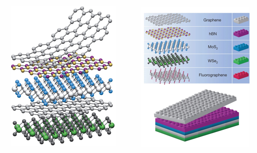
Nanostructures and tailored surfaces play a central role in important technological developments. The electronic, optical and mechanical properties of nanostructures depend not only on the nature of the starting material, but also strongly on the structure size, shape and environment, which can cause quantization of the electronic states along one or more spatial directions.
In this field of study, modern techniques for the targeted fabrication of nanostructures are presented. The physical principles of controlling electronic properties through patterning and dimensionality constraint are taught. Methods for elucidating the morphology, electronic structure, dynamics, and coupling of nanostructures are also introduced. The various scanning probe microscopy methods that can be used to image and modify surfaces at atomic resolution play a major role. Other important techniques such as (time-resolved) optical spectroscopy and (near-field) microscopy are also covered.
Contact person
- Prof. Dr. Ronny Brandenburg
- Prof. Dr. Christian Klinke
- Prof. Dr. Tobias Korn
- Prof. Dr. Sylvia Speller
- Dr. Ingo Barke
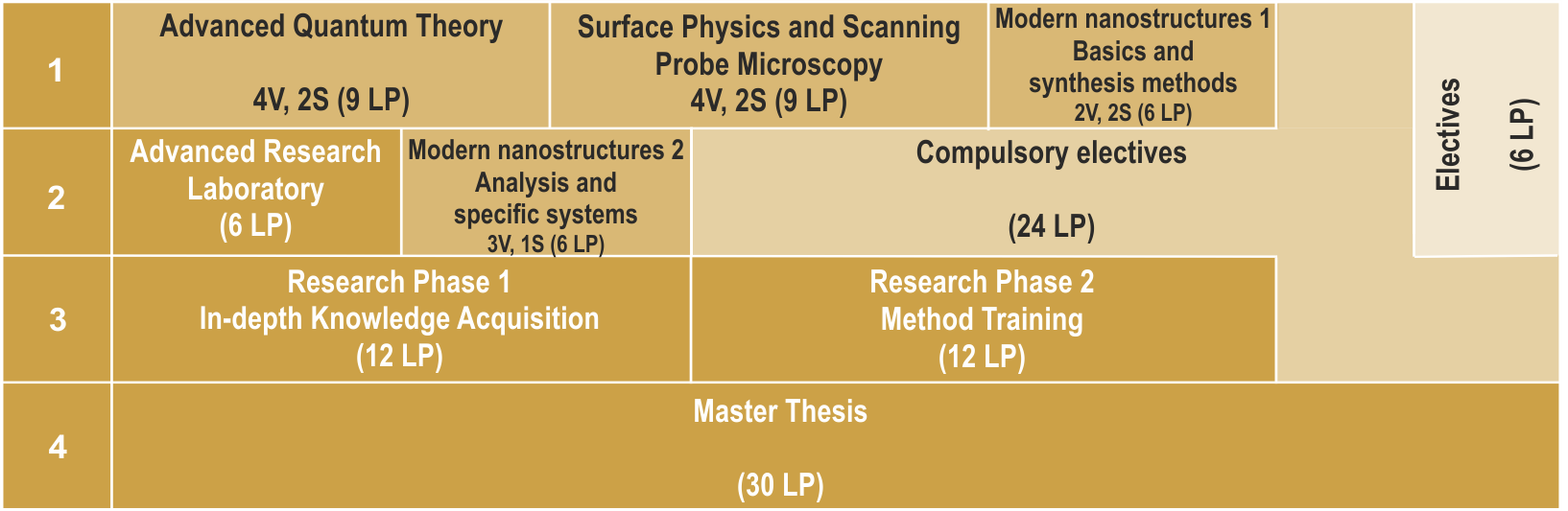
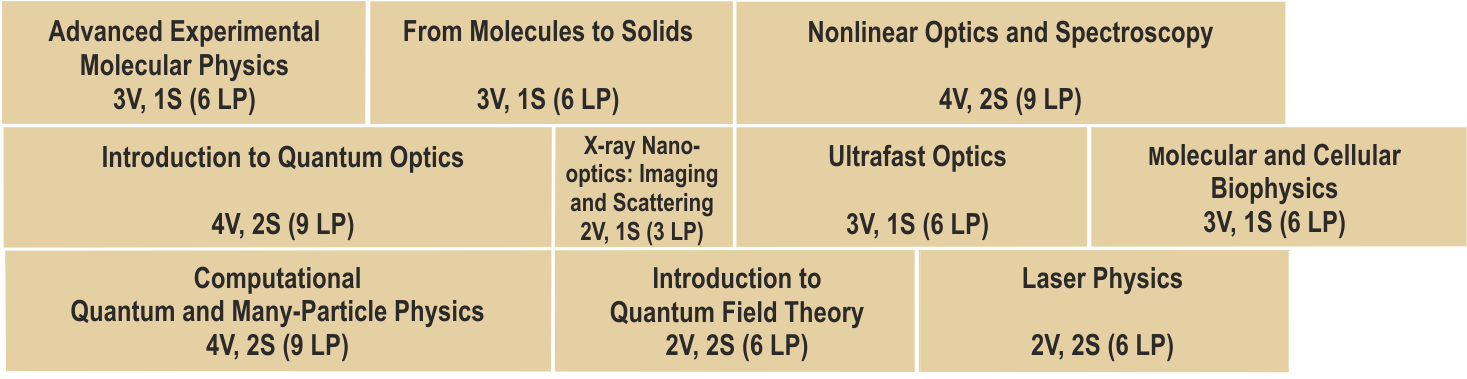
Curriculum